Digital logic Nand gate schematic using inputs outputs when circuit circuitlab created digital stack Xor gate circuit diagram using only nand or nor gate
Schematic and layout of 1X 2-input NAND gates with (a) GLB applied to
[diagram] circuit diagram nand gate Ttl nand explain truth transistors Mos logic cmos nand gate circuits lab4sys implementation
Nand gate circuits integrated
Nand inputs gateInput create using nands nand circuit schematic logic circuitlab created stack Nand gate circuit diagram ic 74ls00 pinout gates logic chip input circuitdigest circuits diagrams working electronic using explanation four limitationsDigital logic.
[diagram] circuit diagram nand gateIntegrated circuits logic gates pdf Cmos nand gate circuit diagramXor nand nor.

Nand cmos pmos nmos logic input transistors nor parallel transistor implementation logica turns switching which quasi delay insensitive gatter function
Energy efficiency in schools: 3 input nand gate stick diagramNand input schematic glb 3 input nand gate circuit diagramNand implementation transistors.
E77 . lab 3 : laying out simple circuitsNand gate diagram Nand gate circuit diagram 2 input diode transistor logicSatish kashyap: microwind tutorial part 5 : three (3) input nand gate.

Gate nand input electronics three logic digital tutorial gates figure above shows
Nand circuit gate diagram input drawPin on elektronica 3 or 4 inputs nand gateIn a 2-input nand, which will be faster when switching: when the a.
Nand gate diagram 74hc00 ttl input quad 7400 pinout latch using gates nor push pull octoprint funny four hasDraw the circuit diagram of ttl nand gate and explain its working with Multisim input nandInput nand gate three microwind stick diagram schematic tutorial part.

How to draw the circuit diagram of 3 input nand gate
Circuit diagram of nand gateSolved: draw a four-input nand gate similar to the five-input gate 74hc00 / 74hct00, quad 2Nand gate diagram.
C-mos logic integrated circuitsNand gate diagram Nand-gate| digital logic gates || electronics tutorialCmos nand gate circuit diagram.
![[DIAGRAM] Uln2003 Logic Diagram - MYDIAGRAM.ONLINE](https://i.ytimg.com/vi/DsPet6URykQ/maxresdefault.jpg)
Digital logic
Nand gate schematic diagramNand logic gates transistor diode nor transistors diodes 5v rtl Nand gate schematic diagram3 input nand gate circuit diagram.
Nand input nor gates logic circuitlabNand layout gate simple figure laying circuits larger version click [diagram] uln2003 logic diagramSchematic and layout of 1x 2-input nand gates with (a) glb applied to.

![[DIAGRAM] Circuit Diagram Nand Gate - MYDIAGRAM.ONLINE](https://i2.wp.com/image2.slideserve.com/5235502/schematic-vs-layout1-l.jpg)
[DIAGRAM] Circuit Diagram Nand Gate - MYDIAGRAM.ONLINE
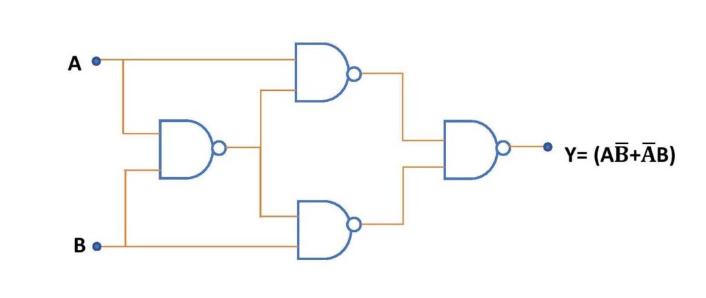
XOR gate circuit diagram using only NAND or NOR gate | Edumir-Physics

Nand Gate Diagram

NAND gate circuit diagram 2 input diode transistor logic | Nand gate

Draw the circuit diagram of TTL NAND gate and explain its working with

C-MOS logic integrated circuits - Lab4Sys.com

transistors - Implementation of NAND gate